Frank Altmann received his Diploma in Physics from the Technical University, Dresden. He joined the Fraunhofer IWM (now IMWS) in 1997 and has since been concerned with material diagnostics and failure analysis as well as with strength and reliability problems of semiconductor components. Since 2006 he has been head of the research group »Diagnostics of semiconductor technologies« with responsibility for national and international research projects with industry and public organizations focusing on Si and GaN chip technologies. Since 2019 he is acting head of the department »Electronic Materials and Components”. Frank Altmann has authored and co-authored more than 60 publications and is active within several national and international failure analysis conference and education committees.
Meet our CAM-Workshop Committee
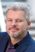
Frank Altmann

Ingrid De Wolf
Ingrid De Wolf received the PhD in Physics from the KU Leuven, Belgium, in 1989. In the same year she joined IMEC, where she worked on microelectronics reliability, with special attention for mechanical stress analysis using micro-Raman spectroscopy and failure analysis. From 1999 to 2014, she headed the group REMO, where research is focused on reliability, test and modelling of 3D technology, interconnect, OIO, MEMS and packaging. She (co-)authored more than 550 publications. She is fellow at IMEC, IEEE senior member, professor at the Department of Materials Engineering of the KU Leuven and program director of the Master of Nanoscience, Nanotechnology and Nanoengineering at the Faculty of Engineering Science at the KU Leuven.
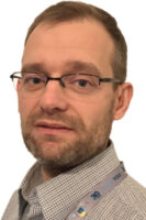
Pascal Gounet
Pascal Gounet received his first diploma of engineering on microelectronics (ISTASE Institut Supérieur des Techniques Avancées Saint Etienne) in 1997. Then he went to the “Ecole des Mines” in Saint Etienne for a second diploma about software engineering received in 1998. He joined STMicroelectronics at the beginning of 1999 first as a designer (analog & digital circuits). He also worked in a CAD software development group. Since 2003, he is engineer in Failure Analysis. Elected in 2011 as physical & circuit edit analyzes expert, he currently works and develops on many topics like (but not limited to) sample preparation, SEM & FIB, microscopy, laser and plasma techniques and technologies.
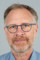
Joerg Krinke
Joerg Krinke received his Diploma in Materials Science from the Friedrich-Alexander- University of Erlangen-Nürnberg in 1995. Prior to joining Robert Bosch GmbH in 2000, he worked as a research associate where his work was mainly concerned with microstructural characterization and electrical behaviour of grain boundaries in polycrystalline Si by the means of EBIC and TEM. Since 2000, Joerg Krinke has worked as an engineer for reliability analyses of active electronic components, later becoming senior expert for reliability and technology assessment of first level packaging technologies of electronic components. Currently he is the Bosch project leader of the publicly sponsored project FA4.0 (Failure Analysis 4.0 – Key for reliable electronic devices in smart mobility and industrial production).
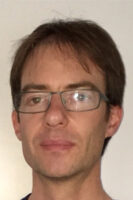
Thomas Schweinboeck
Thomas Schweinboeck received his PhD from University Regensburg (Experimental and Applied Physics, Micro- and Nanostructures). Since 2001, he has been working with Infineon Technologies, Munich, in the Central Failure Analysis Lab, performing electrical and physical analysis for all automotive products within Infineon, during this time also being responsible for method development projects dealing with Scanning Probe and Nano-probing topics. Since 2014, he has been leading a team for failure analysis of MEMS, sensor and bipolar/mixed signal devices. He has authored and co-authored several publications on FA method development and has acted as work package leader for EU funding projects SAM³ and FA4.0.
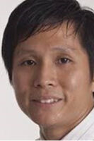
Szu Huat Goh
Szu Huat received his BEng and PhD in electrical and computer engineering from the National University of Singapore. He started his career with GLOBALFOUNDRIES, where he leads a team responsible for product failure diagnostics and advanced methodologies to accelerate yield ramp. He focuses on the development of wafer-level dynamic fault isolation techniques combining with cross-functional domain knowledge of design and test to enhance yield learning. His recent exploration centers on machine learning to enhance FA and yield prediction. He is currently with QUALCOMM yield management team where he is responsible for advanced technologies yield engineering and diagnostic. Szu Huat was the technical program chair, general co-chair and general chair for the International Physical and Failure Analysis (IPFA) in 2016, 2017 and 2018.
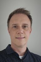
Jeroen Jalink
Jeroen Jalink received his PhD in Physics from the Radboud University Nijmegen in 2014. Thereafter he joined NXP and held several engineering roles in the Product Diagnostic and Quality Center (PDQC), focusing on solder joint and microelectronic reliability (2014-2017), and electrical failure analysis (2017-2021). During this time, he authored and co-authored several publications in these fields. In 2021 he transitioned to the managerial role starting with the Package Analysis Group supporting microelectronic package analysis, material characterization and solder joint reliability. Later that year he became responsible for the overall PDQC Nijmegen organization focusing on Electrical & Physical Failure Analysis, and Material Analysis. Jeroen Jalink is the country coordinator for The Netherlands and co-chair of WP2 in the EU subsidy project FA2IR.
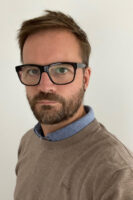
Andreas Meyer
Andreas Meyer studied Applied Physics at the University of Applied Sciences in Zwickau, Germany, where he received his first degree. He went on to study Instrumental Analytical Sciences at the Robert Gordon University in Aberdeen/Scotland receiving a Master of Science degree. In 2000 he joined the Analytical Labs department of AMDs Fab30 in Dresden, Germany. He started his career as Scanning Electron Microscopy engineer working on process development and failure analysis topics of Cu interconnects. During this time he worked on his PhD in the field of electromigration in Cu interconnect.
In 2007 he was awarded a PhD from Brandenburg University of Technology in Cottbus, Germany. Andreas Meyer is currently managing the Fab1 Analytical Labs department as site lead withing the Global Analytical Labs organization of GlobalFoundries. He has given tutorials and hosted sessions at the ISTFA conference at the past.