With more than ten years of experience in microdiagnostics and failure analysis, 3D-Micromac is the industry leader in laser-based sample preparation. Our field-proven microPREP® systems accelerate sample preparation for a wide range of failure analysis methods, including TEM, SEM, APT, XRM, and micromechanical testing. Our latest development, the microPREP® L, can prepare samples on bigger specimens like 12” wafers or system-level boards. These can even be prepared across multiple areas of the same specimen in a single run, without process restarts.
Free your FIB/SEM for what it does best – speed up your time-to-sample with laser-based sample preparation.
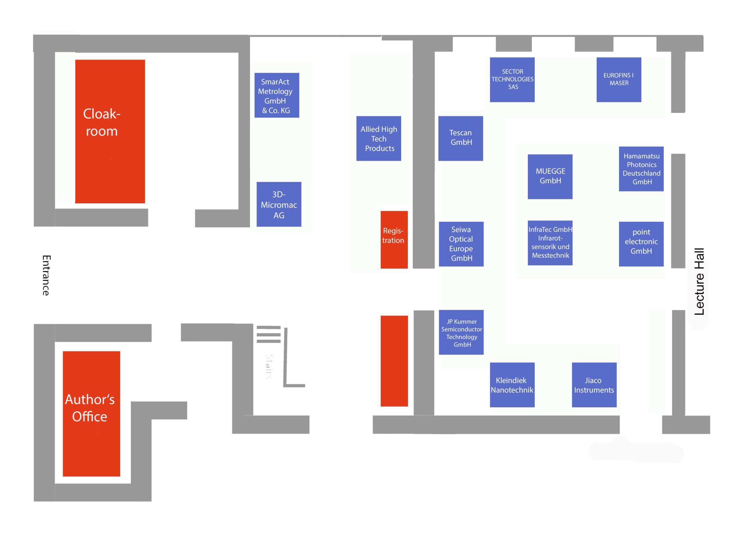
Exhibitors
Please click on the respective exhibitor button below for more information.
3D-Micromac AG
Company Name:
Address:
Website:
Phone:
Email:
3D-Micromac AG
Technologie-Campus 8 I 09126 Chemnitz I Germany
www.3d-micromac.com/
+49 371 40043-907
keller@3d-micromac.com
SmarAct Metrology
SmarAct Metrology develops advanced equipment for high-precision positioning and metrology applications in sectors such as optics, semiconductors, and high-energy research. Our product portfolio spans from miniaturized interferometers for high-resolution displacement measurements to compact optical encoders offering nanometer resolution and high bandwidth for precise motion control.
We also provide turnkey scanning vibrometers for modal analysis of MEMS, compact sensors, and small samples. With full in-house development and production, we deliver highly customized solutions for individual and OEM applications, supported by feasibility studies and comprehensive measurement services.
Company Name:
Address:
Website:
Phone:
Email:
SmarAct Metrology
August-Wilhelm-Kühnholz-Str. 1 I 26135 Oldenburg I Germany
Website: www.smaract.com/metrology
Phone: +49 441 800879 -0
Email: metrology@smaract.com
Allied High Tech Products
For over 43 years, Allied High Tech Products has provided sample preparation products for failure analysis to the microelectronics industry. Allied manufactures cutting-edge equipment at its facilities with all design, manufacturing and assembly taking place in-house to ensure the highest quality equipment is produced. Allied’s state-of-the-art equipment includes the X-Prep® Precision Polishing/Grinding/Milling Machine, MultiPrep™ Polishing System, MetPrep Grinding/Polishing Systems and TechCut™ Sectioning Saws. Please stop by Stand #3 for more in-depth information.
Company Name:
Address:
Website:
Phone:
Email:
Allied High Tech Products, Inc
Carmenita Road 16207 I 90703 Cerritos, California I USA
www.alliedhightech.com
+1 310-635-2466
media@alliedhightech.com

Seiwa Optical Europe GmbH
Seiwa Optical is a Japanese company that has been a provider of customizable optical solutions for machine vision, inspection and industrial processing for over 60 years. We have three factories in Japan, able to manufacture strong lenses for exposure systems, aligners, projection lenses and also design and manufacture tube lens, objective lens such as large image circle objective lens for large sensor size cameras, long working distance high resolution objective lens, IR objective lens for inspection to laser process equipment.
Company Name:
Address:
Website:
Phone:
Email:
Seiwa Optical Europe GmbH
Werrastrasse 8 I 60486 Frankfurt am Main I Germany
www.seiwaeurope.com
+49 6974087847
info@seiwaeurope.com
Tescan GmbH
Tescan, headquartered in Brno, Czech Republic, is a global leader in electron microscopy solutions with a growing focus on the semiconductor industry. Its advanced electron microscopy and ion beam systems enable cutting-edge semiconductor R&D and manufacturing, while also supporting applications in materials and life sciences. During past years Tescan expanded its presence in key APAC markets, including Korea, Singapore, and Taiwan, underscoring its commitment to this vital sector. With over 4,000 SEM installations in 80+ countries and 800 professionals in 16 global locations, Tescan delivers innovative solutions for semiconductor leaders and diverse industries worldwide.
Company Name:
Address:
Website:
Phone:
Email:
Tescan
Zum Lonnenhohl 46 I 44319 Dortmund I Germany
www.tescan.com/applications/semiconductors
0541228563
lucie.brnkova@tescan.com

Sector Technologies
SECTOR TECHNOLOGIES is a specialized distributor of high-end failure analysis equipment for the semiconductor industry.
Our portfolio includes:
# ELECTRICAL FAILURE ISOLATION FROM THERMOFISHER SCIENTIFIC
– Lock-in Thermography (Elite)
– EMMI & Laser Scanning Microscopy and LVI/LVP applications (Meridian family)
– E-beam probing (Meridian EX)
– Nanoprobing solutions (nProber IV, Hyperion)
# SAMPLE PREPARATION
– JetEtch, LaserEtch, and PlasmaEtch – FROM NISENE
– VarioMetric, VarioMill – FROM VARIOSCALE
# ELECTRICAL TEST AND DESIGN DEBUG:
– V550 – FROM TESEDA
– SiC and GaN testing FROM FOCUS TEST
# NIR MICROSCOPY AND OPTICS:
– IR 2200 Microscope and NIR Lenses FROM SEIWA OPTICAL
Company Name:
Address:
Website:
Phone:
Email:
Sector Technologies
rue LAMARTINE 24 I 38320 Eybens I France
sector-technologies.com
+33624024061
antoine.reverdy@sector-technologies.com

Eurofins MASER B.V.
Eurofins MASER is an independent service provider. Since 1993 we have offered Reliability Test and Failure Analysis Services to the semiconductor industry. We offer a wide range of qualification procedures (AEC Q100/JEDEC/etc) to qualify your products according to the latest international standards. Our state-of-the-art Failure Analysis laboratory will fulfill all F/A needs for you. We can support you with your daily Reliability Test or Failure Analysis challenges.
Company Name:
Address:
Website:
Phone:
Email:
Eurofins MASER B.V.
Auke Vleerstraat 26 I 7521PG Enschede I The Netherlands
www.maser.nl
+31657591958
sales@me.eurofinseu.com
Hamamatsu Photonics Deutschland GmbH
HAMAMATSU PHOTONICS is one of a few companies in the world that develops a wide range of light sensors, such as photodiodes, image sensors and photomultiplier tubes, as well as numbers of light sources.
Our portfolio of more than 10,000 products does not only include components, but also fully integrated systems, like our emission microscope PHEMOS®-X for failure localization in semiconductor devices.
Our PHEMOS®-X is designed for the analysis of Memory, Logic, and Power Devices, including advanced technology nodes. It can be equipped with multiple analysis techniques and different detectors. Its structure is flexible to embed each of those approaches, either individually or as “all in one”.
Company Name:
Address:
Website:
Phone:
Email:
Hamamatsu Photonics Deutschland GmbH
Arzbergertstr. 10 I 82211 Herrsching I Germany
www.hamamatsu.de
+49 08152375171
petra.genitheim@hamamatsu.eu
point electronic GmbH
Imina Technologies is a Swiss manufacturer of robotic solutions for electrical characterization under Optical Microscopes, Atomic Force Microscopes, Failure Analysis inspection tools, probe stations, and Scanning Electron Microscopes. These state-of-the-art electrical testing and failure analysis solutions combine precision, stability, and ease of use.
point electronic GmbH is a manufacturer of detectors, acquisition and control systems for SEM, TEM and Micro-analysers. The company is a leader in development of custom electronics for Topography, Electrical Analysis like EBIC and EBAC/RCI, as well as for Electrical Failure Analysis (EFA). point electronic provides complete SEM Modernizations
Company Name:
Address:
Website:
Phone:
Email:
point electronic GmbH / Imina Technologies SA
Erich-Neuß-Weg 15 I 06120 Halle (Saale) I Germany
www.pointelectronic.com
+49 345 1201190
info@pointelectronic.de

Jiaco Instruments
Since 2016, JIACO Instruments’ MIP decapsulation system has set the standard for solving IC decapsulation challenges. As packaging materials grow more complex, new etching challenges arise. To address these, we developed MIP+, extending MIP’s proven capabilities from package-level to die-level etching with:
-New Etching Chemistries: Localized, ion-free solutions for Si, SiO₂ & Si₃N₄
-Unparalleled Versatility: Atmospheric pressure etching of inorganic & organic materials
-Expanded Applications: Selective etching for 2.5D & 3D packages, interposers, and memory
Visit us at booth 10 during CAM Workshop to discover how MIP+ can enhance your analysis and to discuss your decapsulation challenges
Company Name:
Address:
Website:
Phone:
Email:
JIACO Instruments
Feldmannweg 17 I 2628 DW Delft I The Netherlands
jiaco-instruments.com
+31 618416498
info@jiaco-instruments.com
Kleindiek Nanotechnik
Kleindiek Nanotechnik is a leading supplier of nanoprobing and failure analysis tools capable of addressing the most recent technology nodes. Our systems can be integrated into virtually any SEM in the field. Such retrofits are able to transform an existing SEM (or FIB/SEM) into a nanoprobing tool. Once probes have been placed on the device’s contacts, a suite of failure analysis tools including EBIC/EBAC etc, Current Imaging, and Transistor Characterization help operators quickly yield a result. In addition, Kleindiek Nanotechnik offers substages and manipulation tools that enhance operations in SEM and FIB/SEM tools by adding new functionalities.
Company Name:
Address:
Website:
Phone:
Email:
Kleindiek Nanotechnik
Aspenhaustr. 25 I 72770 Reutlingen I Germany
www.kleindiek.com
+49 71213453950
www.kleindiek.com
JP Kummer Semiconductor Technology GmbH
The JP Kummer Semiconductor Technology GmbH is a specialist European Distributor of instruments and consumables mainly for the Semiconductor industry, but also for the Medical Device, Aerospace, Solar and related Industries. We attach great importance to trade with reliable products. We verify the quality of the manufacture of the products sold by us regularly. Our employees are trained in continuous intervals of our suppliers and maintain them with an intensive exchange of information.
Using our long established relationships within these industries worldwide, we bring the newest and most technologically advanced products in their fields to the European market.
Company Name:
Address:
Website:
Phone:
Email:
JP Kummer Semiconductor Technology GmbH
Steinerne Furt 78 I 86167 I Augsburg I Germany
www.jpkummer.eu
+49 82199977390
sales_de@jpkummer.eu

InfraTec GmbH Infrarotsensorik und Messtechnik
InfraTec, with its Infrared Measurement Division, has been one of the world’s leading providers of commercial thermal imaging technology for 35 years. In addition to the high-end ImageIR® camera series, the TarisIR® and VarioCAM® HD product families, the company supplies turnkey thermography automation solutions.
The flexibly configurable E-LIT test system for contactless failure detection and analysis in electrical components consists of an application-specific optimized infrared camera with high-speed lenses, an excitation source, and a motorized X-Y-Z positioning unit. Camera control and data analysis are performed using the associated IRBIS® 3 active thermography software.
Company Name:
Address:
Website:
Phone:
Email:
InfraTec GmbH Infrarotsensorik und Messtechnik
Gostritzer Str. 61-63 I 01217 Dresden I Germany
www.infratec.de
+49 35182876600
web@Infratec.de
MUEGGE GmbH
MUEGGE is a leading international manufacturer of industrial microwave and plasma equipment. Founded in 1986 and headquartered in Reichelsheim Odw., Germany, MUEGGE provides solutions for a wide range of industrial applications for customers in more than 40 countries.
Company Name:
Address:
Website:
Phone:
Email:
MUEGGE GmbH
Hochstraße 4 – 6 I 64385 Reichelsheim I Germany
www.muegge-group.com
+49 616493070
julia.marquardt@muegge.de